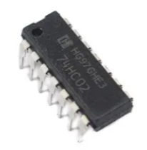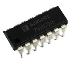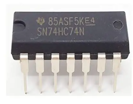
74HC74 LOGIC GATE IC (INTEGRATED CIRCUIT)
KSH 150.00
In Stock
The 74HC74 is a highspeed CMOS logic IC containing two independent Dtype flipflops with set and reset functions. Each flipflop features individual data (D), clock (CP), set (SD), and reset (RD) inputs, along with complementary Q and Q outputs [citation:1]. Data at the D input is transferred to the Q output on the LOWtoHIGH clock transition, making it ideal for frequency division, data storage, shift registers, and synchronizing asynchronous signals [citation:1][citation:7].
| Parameter | Value |
|---|---|
| Supply Voltage (VCC) | 2.0V to 6.0V [citation:3] |
| Input Voltage | 0V to VCC [citation:3] |
| Output Current | ±5.2mA (at 6V) [citation:4] |
| Propagation Delay | 14ns typical (at 5V, CL=15pF) [citation:5] |
| Maximum Clock Frequency | 82MHz [citation:4] |
| Operating Temperature | -40°C to +125°C [citation:1] |
| Package Types | DIP14, SOIC14, TSSOP-14 [citation:1] |
| Number of Flip-Flops | 2 (dual Dtype, positive edgetriggered) |
= Pin Configuration (DIP14/SOIC14/TSSOP-14) =
| Pin | Name | Function |
|---|---|---|
| 1 | 1RD | Flip-Flop 1 Asynchronous Reset (Active LOW) [citation:2] |
| 2 | 1D | Flip-Flop 1 Data Input [citation:2] |
| 3 | 1CP | FlipFlop 1 Clock Input (LOWto-HIGH trigger) [citation:2] |
| 4 | 1SD | Flip-Flop 1 Asynchronous Set (Active LOW) [citation:2] |
| 5 | 1Q | Flip-Flop 1 Normal Output [citation:2] |
| 6 | 1Q | Flip-Flop 1 Complementary Output [citation:2] |
| 7 | GND | Ground (0V) [citation:2] |
| 8 | 2Q | Flip-Flop 2 Complementary Output [citation:2] |
| 9 | 2Q | Flip-Flop 2 Normal Output [citation:2] |
| 10 | 2SD | Flip-Flop 2 Asynchronous Set (Active LOW) [citation:2] |
| 11 | 2CP | FlipFlop 2 Clock Input (LOWto-HIGH trigger) [citation:2] |
| 12 | 2D | Flip-Flop 2 Data Input [citation:2] |
| 13 | 2RD | Flip-Flop 2 Asynchronous Reset (Active LOW) [citation:2] |
| 14 | VCC | Supply Voltage (2V to 6V) [citation:2] |
= Function Table (Per Flip-Flop) =
| Set (SD) | Reset (RD) | Clock (CP) | Data (D) | Q Output | Q Output |
|---|---|---|---|---|---|
| LOW | HIGH | X | X | HIGH | LOW [citation:9] |
| HIGH | LOW | X | X | LOW | HIGH [citation:9] |
| LOW | LOW | X | X | HIGH* | HIGH* [citation:3] |
| HIGH | HIGH | ↑ (Rising) | HIGH | HIGH | LOW [citation:9] |
| HIGH | HIGH | ↑ (Rising) | LOW | LOW | HIGH [citation:9] |
| HIGH | HIGH | LOW | X | No Change | No Change [citation:3] |
*Both outputs HIGH while SD and RD are LOW; output states unpredictable if both go HIGH simultaneously [citation:3].
Two Independent FlipFlops Dual functionality in a single 14-pin package
Asynchronous Set and Reset - Direct control for clearing or presetting outputs
Complementary Outputs - Both Q and Q available for differential signaling
Wide Supply Range - Operates from 2V to 6V for flexible integration
Low Power Consumption 8µA quiescent current ideal for battery-powered designs
High Noise Immunity - CMOS inputs ensure reliable operation in noisy environments
Schmitt Trigger Clock Input - Tolerant to slow clock edges [citation:1]
√ Industry-standard 74HC74 pinout for easy replacement
√ Low power consumption - 8µA typical quiescent current
√ Fully tested and guaranteed functional