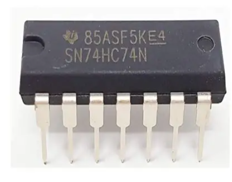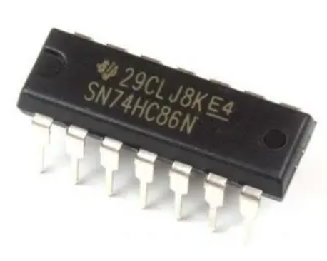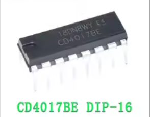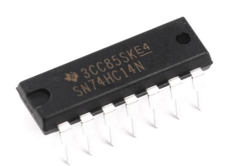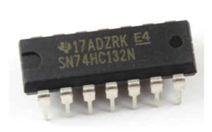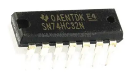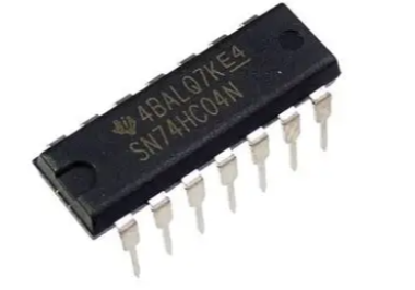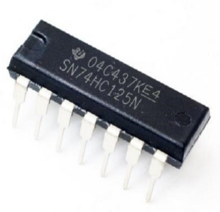
74HC125 LOGIC GATE IC (INTEGRATED CIRCUIT)
KSH 150.00
In Stock
The 74HC125 is a highspeed CMOS logic IC featuring four independent buffer gates with 3state outputs[citation:4][citation:7]. Each noninverting buffer has a separate activelow output enable (nOE) pin. Driving this pin HIGH places the output in a highimpedance (OFF) state, effectively disconnecting the buffer from the bus and allowing multiple devices to share the same line without conflict[citation:4][citation:10][citation:6]. This makes the 74HC125 ideal for memory address drivers, clock drivers, and other busoriented systems[citation:2].
| Parameter | Value |
|---|---|
| Supply Voltage (VCC) | 2.0V to 6.0V[citation:4] |
| Input Voltage | 0V to VCC[citation:9] |
| Output Current (High/Low) | ±7.8mA (at 6V)[citation:4] |
| Propagation Delay | 9ns typical at 5V[citation:12] |
| Quiescent Current | 8µA typical[citation:12] |
| Operating Temperature | -40°C to +125°C[citation:4] |
| Package Types | DIP14, SOIC14, TSSOP-14[citation:5][citation:4] |
| Number of Gates | 4 (non-inverting buffers)[citation:4] |
= Pin Configuration (DIP14/SOIC14/TSSOP-14) =
| Pin | Name | Function |
|---|---|---|
| 1 | 1OE | Channel 1 Output Enable (Active LOW)[citation:3] |
| 2 | 1A | Channel 1 Data Input[citation:3] |
| 3 | 1Y | Channel 1 Data Output[citation:3] |
| 4 | 2OE | Channel 2 Output Enable (Active LOW)[citation:3] |
| 5 | 2A | Channel 2 Data Input[citation:3] |
| 6 | 2Y | Channel 2 Data Output[citation:3] |
| 7 | GND | Ground (0V)[citation:3] |
| 8 | 3Y | Channel 3 Data Output[citation:3] |
| 9 | 3A | Channel 3 Data Input[citation:3] |
| 10 | 3OE | Channel 3 Output Enable (Active LOW)[citation:3] |
| 11 | 4Y | Channel 4 Data Output[citation:3] |
| 12 | 4A | Channel 4 Data Input[citation:3] |
| 13 | 4OE | Channel 4 Output Enable (Active LOW)[citation:3] |
| 14 | VCC | Supply Voltage (2V to 6V)[citation:3] |
= Truth Table (Per Buffer) =
| Input (nA) | Enable (nOE) | Output (nY) |
|---|---|---|
| X | HIGH | Z (High-Impedance)[citation:10] |
| LOW | LOW | LOW[citation:2] |
| HIGH | LOW | HIGH[citation:2] |
= Key Features =
3State Outputs Enables shared bus connections without conflict[citation:2]
Four Independent Buffers Multiple channels in a single 14pin package[citation:4]
Wide Supply Range - Operates from 2V to 6V for flexible integration[citation:6]
Low Power Consumption 8µA quiescent current ideal for battery-powered devices[citation:12]
High Noise Immunity - CMOS inputs ensure reliable operation in noisy environments[citation:2]
Schmitt Trigger Action - Clean switching even with slow input edges[citation:6]
15 LSTTL Load Drive Capable of driving 15 lowpower Schottky TTL loads[citation:2]
√ Compatible with CMOS, NMOS, and TTL logic levels[citation:2]
√ Industry-standard 74HC125 pinout for easy replacement
√ RoHS compliant and green device options available[citation:6]